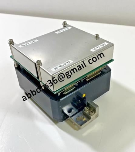
HAMAMATSU C8779K-01 scanning unit
Руководство по продукту:
HAMAMATSU C8779K-01 scanning unit
Введение: HAMAMATSU C8779K-01 Hamamatsu Optical Scanning Unit has high imaging accuracy and stable scanning, suitable for continuous inspection operations of semiconductor wafer appearance inspection equipment.
High precision optical scanning optical path, clear identification of subtle defects
Anti stray light design for optical path, interference free imaging in workshop environment
Built in overload and over temperature circuit protection, extending the service life
Standardized overall module, easy disassembly, обслуживание, и замена
Indicator lights distinguish between standby, scanning, and abnormal alarm states
Original factory equipped Hamamatsu detection optical system with high adaptability
High speed continuous scanning, smooth detection rhythm without lagging
Power on automatic optical path self-test, quickly locate optical path faults
Industrial standard power supply, suitable for dust-free constant temperature testing workshop
Compact integrated module, saving equipment installation space
Sealed dust-proof structure, suitable for clean factory working conditions
Stable data transmission interface, compatible with the main control image processing system
Built in parameter storage, no need to readjust when switching detection samples
Automatically record scan exception logs for easy maintenance and troubleshooting
Precision optical components with minimal long-term performance degradation
Заключение: This scanning unit has precise imaging, пыленепроницаемость, durability, and easy maintenance, making it a core replacement spare part for semiconductor optical defect detection equipment.
Подробные фотографии продукта:
видео о продукте
Другие ссылки
TRICONEX 3009监测模块
ALSTOM EP3-E-4-A控制器
GE 8502-BI-DP总线接口模块
Другие ссылки
Heuft HBE010200 Control Terminal Card
DA501 Analog I/O Module
SIEMENS 6GK1143-0TB01 Industrial Control System